Markets
Semiconductor Test Board
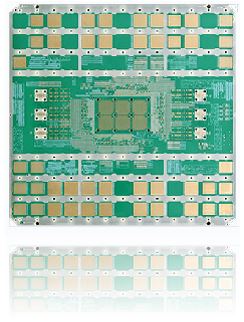
Load Board
The load board is used to connect test unit of testing devices and the physical circuit interfaces of device under test (Abbr. DUT). It can be fixed on probe test console, handler, or other testing hardwares. The wires of load board are connected to probe of internal signal test card of test machine and pins of the DUT.
The load board is mainly used in testing yield after back-end IC packaging of semiconductor. The testing in this phase aims to sorting ICs with incomplete functions, thereby further ensuring IC quality of avoiding product scrapping due to detective ICs. The models include 93K, T2000, and TUF series.
| Item | Value |
| PCB Technoloyg |
Hybird |
| Available Raw Material | SYL+Rogers (S1000-2M+4350B) |
| Layer Count | 8 |
| Board Thickness mm | 2.0 |
| Finish Copper | 35um |
| Line Width/Space | 2.8/2.8mil |
| Surface Finish | Immersion Gold |
| Speical Request | Resin pluging and capped |
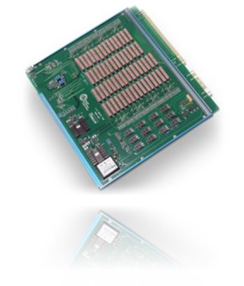
Burn in board (Abbr. BIB)
The burn in board (Abbr. BIB) is used to carry out aging tests in a specific operating condition and time period, for ICs that have completed packaging tests, to verify reliability of ICs.
It connects the ICs for testing by sockets or IC mounts, and testing will be conducted in the oven to repeately test many conditions (HTOL, HAST, etc.), such as temperature, voltage and signals. The bath-tube curve will be determined to pick out the flawed electronic components at the early and late stages.
| Item |
Value |
| PCB Technoloyg | Rigid |
| Available Raw Material | ITEQ IT180A; Ventec VT-901 |
| Layer Count | 8~30 |
| Board Thickness mm | 5.35 |
| Finish Copper | 35um |
| Line Width/Space | 2.8/2.8mil |
| Surface Finish | Immersion Gold; EPENIG |
| Speical Request | Resin pluging and capped ,contersinks |
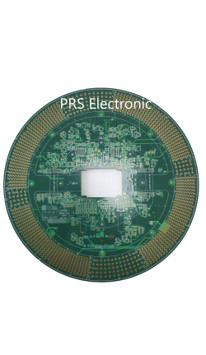
Logic IC Probe Card
For the purpose of conducting various kinds of IC testing, the load board is used as an interface between IC for testing and the automatic test equipment (Abbr. ATE) to transmit electricity and signal. Hence, the signal integrity (Abbr. SI) and power integrity (Abbr. PI) of load board design should be strictly inspected to avoid wrong testing results of IC functions.
| Item |
Value |
| PCB Technoloyg | Rigid |
| Available Raw Material | ITEQ IT180A; Ventec VT-901 |
| Layers | 38L Max |
| Board Thickness mm | 7.0 |
| Finish Copper | 35um |
| Line Width/Space | 2.8/2.8mil |
| Surface Finish | EPENIG; Flash Gold+Hard Gold |
| Speical Request | Resin pluging and capped , contersinks |